MicroMax's Solutions
MicroMax's Solutions
MicroMax's Solutions
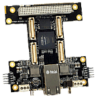 FPGA-PCI104
Building platforms supporting the Altera Cyclone FPGA
The FPGA-PCI104 is a building platform that supports up to four daughter cards. Each daughter card location supports interfaces with up to 28 I/O signals. Each daughter card location is symmetrical. Daughter cards can encompass one or more daughter card locations for greater I/O. For example, the FPDB-DEV uses all four daughter card locations and has access to 104 I/O signals.
The FPGA-PCI104 is PCI-104 compliant and has a full PCI 2.2 interface. The on-board FPGA is configured via the on-board EEPROM, ISA/ PCI bus, or the JTAG port. The configuration EEPROM can be programmed, independently of the FPGA, over the PCI-104 bus or via the ISP port.
The FPGA-PCI104 is based on the Altera’s Cyclone FPGA family: 4K, 12K or 20K logic element parts. Altera’s free Quartus-II basic FPGA design software can be used by the end-user to define the circuit/system functions to be implemented in the on-board FPGA.
The FPGA-PCI104 have an on-board real-time counter/clock with SuperCap backup, and a unique read-only 64-bit serial number ROM. Included on the FPGA-PCI104 are the connectors and physical layer circuits for a I2C/SMBus. Also included are a 60 MHz oscillator, and an SMB connector for an external reference frequency source.
The FPGA-PCI104 is powered from the PCI bus, or external 6V DC to 18V DC supply. Temperature range is 0°C to 85°C.
FPGA-PCI104
Building platforms supporting the Altera Cyclone FPGA
The FPGA-PCI104 is a building platform that supports up to four daughter cards. Each daughter card location supports interfaces with up to 28 I/O signals. Each daughter card location is symmetrical. Daughter cards can encompass one or more daughter card locations for greater I/O. For example, the FPDB-DEV uses all four daughter card locations and has access to 104 I/O signals.
The FPGA-PCI104 is PCI-104 compliant and has a full PCI 2.2 interface. The on-board FPGA is configured via the on-board EEPROM, ISA/ PCI bus, or the JTAG port. The configuration EEPROM can be programmed, independently of the FPGA, over the PCI-104 bus or via the ISP port.
The FPGA-PCI104 is based on the Altera’s Cyclone FPGA family: 4K, 12K or 20K logic element parts. Altera’s free Quartus-II basic FPGA design software can be used by the end-user to define the circuit/system functions to be implemented in the on-board FPGA.
The FPGA-PCI104 have an on-board real-time counter/clock with SuperCap backup, and a unique read-only 64-bit serial number ROM. Included on the FPGA-PCI104 are the connectors and physical layer circuits for a I2C/SMBus. Also included are a 60 MHz oscillator, and an SMB connector for an external reference frequency source.
The FPGA-PCI104 is powered from the PCI bus, or external 6V DC to 18V DC supply. Temperature range is 0°C to 85°C.
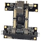 FPGA104
Building platform: supporting Altera Cyclone FPGA
The FPGA104 is a building platform that support up to four daughter cards. Each daughter card location supports interfaces with up to 28 I/O signals. Each daughter card location is symmetrical. Daughter cards can encompass one or more daughter card locations for greater I/O. For example, the FPDB-DEV uses all four daughter card locations and has access to 104 I/O signals.
The FPGA104 is PC/104 compliant and is interfaced to the full PC/104 bus signals including memory and I/O mapped signals. The on-board FPGA is configured via the on-board EEPROM, ISA bus, or the JTAG port. The configuration EEPROM can be programmed, independently of the FPGA, over the PC/104 bus or via the ISP port.
The FPGA104 is a based on the Altera’s Cyclone FPGA family: 4K, 12K or 20K logic element parts. Altera’s free Quartus-II basic FPGA design software can be used by the end-user to define the circuit/system functions to be implemented in the on-board FPGA.
The FPGA104 have an on-board real-time counter/clock with SuperCap backup, and a unique read-only 64-bit serial number ROM. Included on the FPGA104 are the connectors and physical layers circuits for a I2C/SMBus, a 50 MHz oscillator, and an SMB connector for an external reference frequency source. The FPGA104 is powered from the ISA bus, or external 6V DC to 18V DC supply.
Temperature range is 0°C to 85°C.
FPGA104
Building platform: supporting Altera Cyclone FPGA
The FPGA104 is a building platform that support up to four daughter cards. Each daughter card location supports interfaces with up to 28 I/O signals. Each daughter card location is symmetrical. Daughter cards can encompass one or more daughter card locations for greater I/O. For example, the FPDB-DEV uses all four daughter card locations and has access to 104 I/O signals.
The FPGA104 is PC/104 compliant and is interfaced to the full PC/104 bus signals including memory and I/O mapped signals. The on-board FPGA is configured via the on-board EEPROM, ISA bus, or the JTAG port. The configuration EEPROM can be programmed, independently of the FPGA, over the PC/104 bus or via the ISP port.
The FPGA104 is a based on the Altera’s Cyclone FPGA family: 4K, 12K or 20K logic element parts. Altera’s free Quartus-II basic FPGA design software can be used by the end-user to define the circuit/system functions to be implemented in the on-board FPGA.
The FPGA104 have an on-board real-time counter/clock with SuperCap backup, and a unique read-only 64-bit serial number ROM. Included on the FPGA104 are the connectors and physical layers circuits for a I2C/SMBus, a 50 MHz oscillator, and an SMB connector for an external reference frequency source. The FPGA104 is powered from the ISA bus, or external 6V DC to 18V DC supply.
Temperature range is 0°C to 85°C.
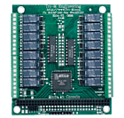 R104
Optoisolated Input and replay Output Board
R104-16DI and R104-16DO
· Relay Output Control The 16 inputs are accessed through I/O memory reads. The inputs are grouped in sets of four, and the group I/O memory address is an offset from the base decode address.
R104-16DO
· Relay Output Control
The 8 relays are accessed through I/O memory writes. The relays are grouped in sets of four, and the group I/O memory address is an offset from the base decode address.
R104
Optoisolated Input and replay Output Board
R104-16DI and R104-16DO
· Relay Output Control The 16 inputs are accessed through I/O memory reads. The inputs are grouped in sets of four, and the group I/O memory address is an offset from the base decode address.
R104-16DO
· Relay Output Control
The 8 relays are accessed through I/O memory writes. The relays are grouped in sets of four, and the group I/O memory address is an offset from the base decode address.
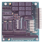 Opal-MM
Optoisolated Input + Relay Output PC/104 Module
Opal-MM is a PC/104 format digital I/O module designed for industrial applications requiring isolation between the computer and the external signals it is monitoring and controlling. This module features 8 optoisolated digital inputs and 8 relay outputs. Each input can accept both AC and DC voltages as low as 3V and as high as 24V.
Opal-MM
Optoisolated Input + Relay Output PC/104 Module
Opal-MM is a PC/104 format digital I/O module designed for industrial applications requiring isolation between the computer and the external signals it is monitoring and controlling. This module features 8 optoisolated digital inputs and 8 relay outputs. Each input can accept both AC and DC voltages as low as 3V and as high as 24V.
 TMX32
Analog Front-End Board
Input-Expansion Board with Thermocouple Compensation.
TMX32
Analog Front-End Board
Input-Expansion Board with Thermocouple Compensation.
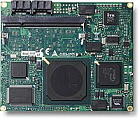
 ETX-NR667
ETX module
The ETX-NR667s CPU scales from a ULV Intel Celeron up to an Intel Core 2 Duo that allows it to be used in both average performance applications, that require very low power, and in applications that need high speed with high-end graphics support. The module has one SODIMM socket that can accommodate a maximum of 2 GB of DDR2 memory. Graphics support on the module includes single- or dual-channel 24-bit LVDS, Analog CRT and TV-out (SDTV and HDTV). The module further incorporates an Intel based 10/100Base-T Ethernet port, a PATA EIDE controller, a dual-port SATA controller, four USB v2.0 ports, two serial ports, one parallel port (SPP/ECP/EPP) shared with FDD, one PS/2 keyboard/mouse interface, an AC97 audio interface, and power management functionality. The ETX-NR667 fully supports PCI and legacy ISA and comes with embedded features such as Watchdog controller, RS-232 console redirection and CMOS EEPROM backup for BIOS settings and battery-less operation.
ETX-NR667
ETX module
The ETX-NR667s CPU scales from a ULV Intel Celeron up to an Intel Core 2 Duo that allows it to be used in both average performance applications, that require very low power, and in applications that need high speed with high-end graphics support. The module has one SODIMM socket that can accommodate a maximum of 2 GB of DDR2 memory. Graphics support on the module includes single- or dual-channel 24-bit LVDS, Analog CRT and TV-out (SDTV and HDTV). The module further incorporates an Intel based 10/100Base-T Ethernet port, a PATA EIDE controller, a dual-port SATA controller, four USB v2.0 ports, two serial ports, one parallel port (SPP/ECP/EPP) shared with FDD, one PS/2 keyboard/mouse interface, an AC97 audio interface, and power management functionality. The ETX-NR667 fully supports PCI and legacy ISA and comes with embedded features such as Watchdog controller, RS-232 console redirection and CMOS EEPROM backup for BIOS settings and battery-less operation.
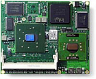 ETX-IM333
ETX module
ETX-IM333 is based on the Intels embedded 855GME Northbridge and ICH4 Southbridge. It supports Celeron M and Pentium M (Banias/Dothan) CPUs in the range of 600MHz to 2.0GHz. The CPU / Chipset combination is ideal for applications that require high performance, reliability, and long product availability. The Intel 855GME Chipset graphics memory controller hub (GMCH-M) provides integrated graphics (250MHz) capabilities and power saving features. The 855GME Northbridge incorporates a DDR memory controller and supports DDR333 in addition to DDR266/200 memory for up to 1GB in a single 200-pin SODIMM socket. Graphic support for CRT and single/dual channel LVDS is included. Optionally, the board can support TV 0ut (SDTV and HDTV). The integrated EIDE controller supports both PIO and UDMA modes, USB ports v2.0, two serial ports, one parallel port (SPP/ECP/EPP), one PS2 keyboard/mouse interface, AC97 audio interface, Fast Ethernet LAN controller, and power management functionality.
ETX-IM333
ETX module
ETX-IM333 is based on the Intels embedded 855GME Northbridge and ICH4 Southbridge. It supports Celeron M and Pentium M (Banias/Dothan) CPUs in the range of 600MHz to 2.0GHz. The CPU / Chipset combination is ideal for applications that require high performance, reliability, and long product availability. The Intel 855GME Chipset graphics memory controller hub (GMCH-M) provides integrated graphics (250MHz) capabilities and power saving features. The 855GME Northbridge incorporates a DDR memory controller and supports DDR333 in addition to DDR266/200 memory for up to 1GB in a single 200-pin SODIMM socket. Graphic support for CRT and single/dual channel LVDS is included. Optionally, the board can support TV 0ut (SDTV and HDTV). The integrated EIDE controller supports both PIO and UDMA modes, USB ports v2.0, two serial ports, one parallel port (SPP/ECP/EPP), one PS2 keyboard/mouse interface, AC97 audio interface, Fast Ethernet LAN controller, and power management functionality.
 ETX-IM266
ETX module
ETX-IM266 is based on the Intels embedded 852GM Northbridge and ICH4 Southbridge. It supports Celeron M CPUs in the range of 600MHz to 1.5GHz. The CPU / Chipset combination is ideal for applications that require average performance, low cost, reliability, and long product availability. The Intel 852GM Chipset graphics memory controller hub (GMCH-M) provides integrated graphics (250MHz) capabilities and power saving features. The 852GM Northbridge incorporates a DDR memory controller and supports DDR266/200 memory for up to 1GB in a single 200-pin SODIMM socket. Graphic support for CRT and single/dual channel LVDS is included. Optionally, the board can support TV 0ut (SDTV and HDTV). The integrated EIDE controller supports both PIO and UDMA modes, USB ports v2.0, two serial ports, one parallel port (SPP/ECP/EPP), one PS2 keyboard/mouse interface, AC97 audio interface, Fast Ethernet LAN controller, and power management functionality.
ETX-IM266
ETX module
ETX-IM266 is based on the Intels embedded 852GM Northbridge and ICH4 Southbridge. It supports Celeron M CPUs in the range of 600MHz to 1.5GHz. The CPU / Chipset combination is ideal for applications that require average performance, low cost, reliability, and long product availability. The Intel 852GM Chipset graphics memory controller hub (GMCH-M) provides integrated graphics (250MHz) capabilities and power saving features. The 852GM Northbridge incorporates a DDR memory controller and supports DDR266/200 memory for up to 1GB in a single 200-pin SODIMM socket. Graphic support for CRT and single/dual channel LVDS is included. Optionally, the board can support TV 0ut (SDTV and HDTV). The integrated EIDE controller supports both PIO and UDMA modes, USB ports v2.0, two serial ports, one parallel port (SPP/ECP/EPP), one PS2 keyboard/mouse interface, AC97 audio interface, Fast Ethernet LAN controller, and power management functionality.
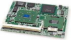
 ETX-GLX
ETX module
AMD Geode LX800 ETX module with USB 2.0 and SATA.
ETX-GLX
ETX module
AMD Geode LX800 ETX module with USB 2.0 and SATA.
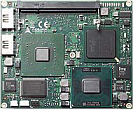
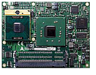 Express-DW400
COM Express module
The Express-DW400 is based on Intel Core 2 Duo and Core Duo CPUs, in the range of 1.06 Ghz up to 2.1 GHz, and the Intel 3100, that is an integrated chip containing the functionality of both a Memory Controller Hub and an I/O Controller Hub. The Intel 3100 Chipset provides a x8 PCI Express interface that may alternatively be configured as two independent x4 PCI Express interfaces in addition it support four x1 PCI Express interfaces. The Intel 3100 Chipset includes an integrated four-channel Enhanced Direct Memory Access (EDMA) controller to perform background data transfers between locations in main memory, or from main memory to a memory-mapped I/O destination. It supports registered ECC type, single channel DDR2 400MHz memory. The module is either available with two vertical placed SODIMM sockets or with one horizontal placed SODIMM socket for a maximum of up to 4 GB system memory.
Express-DW400
COM Express module
The Express-DW400 is based on Intel Core 2 Duo and Core Duo CPUs, in the range of 1.06 Ghz up to 2.1 GHz, and the Intel 3100, that is an integrated chip containing the functionality of both a Memory Controller Hub and an I/O Controller Hub. The Intel 3100 Chipset provides a x8 PCI Express interface that may alternatively be configured as two independent x4 PCI Express interfaces in addition it support four x1 PCI Express interfaces. The Intel 3100 Chipset includes an integrated four-channel Enhanced Direct Memory Access (EDMA) controller to perform background data transfers between locations in main memory, or from main memory to a memory-mapped I/O destination. It supports registered ECC type, single channel DDR2 400MHz memory. The module is either available with two vertical placed SODIMM sockets or with one horizontal placed SODIMM socket for a maximum of up to 4 GB system memory.
